When you think about cutting edge technology, perhaps AI or quantum computing springs to mind. But often, the most important work happens at a much smaller scale: controlling atomic-level processes in semiconductor manufacturing. This is the core of modern electronics, specifically in techniques like Atomic Layer Etching (ALE) and Atomic Layer Deposition (ALD), where precise ion manipulation is key.
Previously, controlling the energy of ions hitting a wafer has been tricky. Regular DC voltage can give you ideal, uniform ion energies (monoenergetic), but it causes charge build-up on the wafer, blocking control. Sinusoidal waveforms which are smooth, repeating waves, prevent this charging, but they create messy, multi-peaked ion energy distributions.
This is where tailored waveforms come in. These custom energy pulses are designed to solve both problems by discharging dielectric surfaces (stopping charge build-up!) and creating nearly uniform ion energy distributions. Their secret is a specific structure: a quick positive phase to attract electrons, followed by a longer negative phase that accelerates ions. Crucially, this negative phase includes a negative slope in the voltage, essential for properly discharging the wafer.

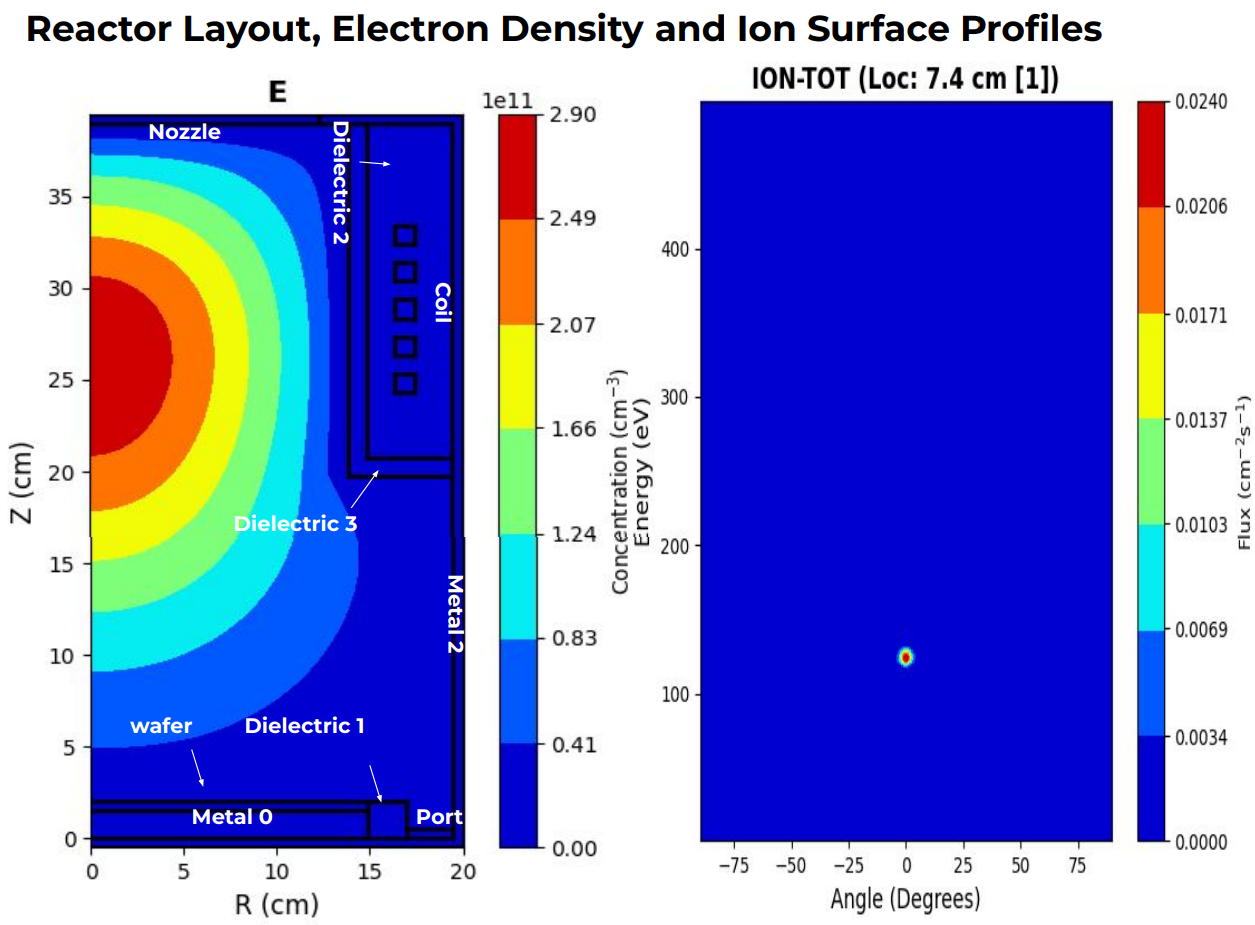
Quantemol’s leading scientists Sebastian Mohr and Hyungseon Song have been researching the topic. They are currently attempting to replicate experimental results. Initial simulations, which did not include a slope, demonstrated that wafer conductivity influences ion energy. This finding highlights the need for more complex waveforms including a slope that depends on wafer conductivity. Further research will involve adjusting the slope and will lead to simulations which can be used to find the necessary slope for a given wafer material.
Previous work[1] found that the voltage slope within the waveform is key. When charges are managed, there’s a direct link between the mean ion energy and the electric field slope. This offers a predictable way to control ion energy. Quantemol scientists studied how the voltage slop removes the charging effect. Also, how it is possible that the electric field can enter into the plasma, which in turn accelerates ions so they have mono-energy (same energy).
These findings highlight the huge potential of tailored waveforms for advanced plasma processing. They are proving the principle of ion mono-energy control with tailored wave-forms, and show how the voltage slope is crucial for discharging materials. By changing the DC voltage, they can control the average ion energy, which makes it flexible for different ALE energy ranges.
This isn’t just academic curiosity, it’s foundational to building the next generation of semiconductor devices. By mastering ion energy control, we’re shaping the future of electronics, one atom at a time.
CLICK HERE to see the full scientific breakdown from our experts. Make sure to follow us on linkedIn to stay up to date with our most recent content.
By Annie Laver, Sebastian Mohr, and Hyungseon Song

Annie Laver
COMMUNICATIONS ADMINISTRATOR

Dr Sebastian Mohr
CHIEF TECHNOLOGY OFFICER

Dr Hyungseon Song
COMPUTATIONAL PLASMA SCIENTIST
References:
[1] Faraz et al, J. Appl. Phys. 128, 213301 (2020)
