Quantemol Virtual Tool: Expert Plasma Simulation
Q-VT is an expert software for simulating industrial plasma processing tools. It uses the validated HPEM code developed by Professor Mark Kushner and his group (University of Michigan), ideal for low-pressure (< 1 Torr) plasmas.

Quantemol Virtual Tool: Expert Plasma Simulation
Q-VT is an expert software for simulating industrial plasma processing tools. It uses the validated HPEM code developed by Professor Mark Kushner and his group (University of Michigan), ideal for low-pressure (< 1 Torr) plasmas.

Quantemol Virtual Tool: Expert Plasma Simulation
Q-VT is an expert software for simulating industrial plasma processing tools. It uses the validated HPEM code developed by Professor Mark Kushner and his group (University of Michigan), ideal for low-pressure (< 1 Torr) plasmas.

Proven Accuracy
Experimentally validated for plasma tools, ensuring the reliability of your simulations.

Streamlined Operations
Multi-run management for efficient batch processing of your simulations.

Comprehensive Data
Includes validated plasma chemistries & cross-sections for accurate modelling.
Effortless Design
Easy chamber design tool (setup service available) simplifies your workflow.
Expanded Capabilities
Model complex phenomena with optional modules for deeper insights.
Integrated Analysis
Import experimental results for seamless comparison and validation.
Scalable Power
Easy job distribution on clusters for faster and more powerful computations.

Insightful Views
Advanced visualisation (scalar & vector) helps you interpret your data.
Proven Accuracy
Experimentally validated for plasma tools, ensuring the reliability of your simulations.

Streamlined Operations
Multi-run management for efficient batch processing of your simulations.

Comprehensive
Data
Includes validated plasma chemistries & cross-sections for accurate modelling.
Effortless Design
Easy chamber design tool (setup service available) simplifies your workflow.
Expanded Capabilities
Model complex phenomena with optional modules for deeper insights.
Integrated Analysis
Import experimental results for seamless comparison and validation.
Scalable Power
Easy job distribution on clusters for faster and more powerful computations.

Insightful Views
Advanced visualisation (scalar & vector) helps you interpret your data.
Proven Accuracy
Experimentally validated for plasma tools, ensuring the reliability of your simulations.

Streamlined Operations
Multi-run management for efficient batch processing of your simulations.

Comprehensive Data
Includes validated plasma chemistries & cross-sections for accurate modelling.
Effortless Design
Easy chamber design tool (setup service available) simplifies your workflow.
Expanded Capabilities
Model complex phenomena with optional modules for deeper insights.
Integrated Analysis
Import experimental results for seamless comparison and validation.
Scalable Power
Easy job distribution on clusters for faster and more powerful computations.

Insightful Views
Advanced visualisation (scalar & vector) helps you interpret your data.
 Complex Electromagnetic Plasma Interactions
Including Current coils, permanent magnents, multi-frequency power supplies and plasma circuit interactions .
 Plasma Tool Geometry Alterations
 Advanced Volume and Surface Chemistries
 Non-Maxwellian Electron Dynamis
 Fluctuations of Plasma State variables and Parameter changes
 Ion Flux on Wafer Level
Including ion energy or angular distribution functions & fluxes of all species on the wafer
 Complex Electromagnetic Plasma Interactions
Including Current coils, permanent magnents, multi-frequency power supplies and plasma circuit interactions .
 Plasma Tool Geometry Alterations
 Advanced Volume and Surface Chemistries
 Non-Maxwellian Electron Dynamis
 Fluctuations of Plasma State variables and Parameter changes
 Ion Flux on Wafer Level
Including ion energy or angular distribution functions & fluxes of all species on the wafer
 Complex Electromagnetic Plasma Interactions
Including Current coils, permanent magnents, multi-frequency power supplies and plasma circuit interactions .
 Plasma Tool Geometry Alterations
 Advanced Volume and Surface Chemistries
 Non-Maxwellian Electron Dynamis
 Fluctuations of Plasma State variables and Parameter changes
 Ion Flux on Wafer Level
Including ion energy or angular distribution functions & fluxes of all species on the wafer
QVT Applications →
✅ Tool design & development.
✅ Model discharge & wafer chemistry.
✅ Analyse etch/deposition uniformity.
✅ Examine tilting effects (with profile models).
✅ Simulate large wafers (12 inches+).
QVT Applications →
✅ Tool design & development.
✅ Model discharge & wafer chemistry.
✅ Analyse etch/deposition uniformity.
✅ Examine tilting effects (with profile models).
✅ Simulate large wafers (12 inches+).
QVT Applications →
✅ Tool design & development.
✅ Model discharge & wafer chemistry.
✅ Analyse etch/deposition uniformity.
✅ Examine tilting effects (with profile models).
✅ Simulate large wafers (12 inches+).
‘Trusted by Scientists Worldwide’
In the core engine of Quantemol-VT lies a powerful Hybrid Plasma Equipment Model (HPEM) code. This code has a proven track of publications, validating it with experimental data and other methods. Here you can find some publications in relevant sections, which seem to be frequently asked about.
QVT Validation ↓
Model overview:
Mark J Kushner “Hybrid modelling of low temperature plasmas for fundamental investigations and equipment design” 2009 J. Phys. D: Appl. Phys. 42 194013
ICP
M Mao and A Bogaerts, “Investigating the plasma chemistry for the synthesis of carbon nanotubes/nanofibres in an inductively coupled plasma enhanced CVD system: the effect of different gas mixtures.” J. Phys. D: Appl. Phys. 43 (2010)
Ken Tokashiki et al, “Synchronous Pulse Plasma Operation upon Source and Bias Radio Frequencys for Inductively Coupled Plasma for Highly Reliable Gate Etching Technology” Jpn. J. Appl. Phys. 48, 2009
S Tinck et al “Simulation of an Ar/Cl2 inductively coupled plasma: study of the effect of bias, power and pressure and comparison with experiments” J. Phys. D: Appl. Phys. 41, 2008
Shu-Xia Zhao et al “Gas ratio effects on the Si etch rate and profile uniformity in an inductively coupled Ar/CF4 plasma.” Plasma Sources Sci. Technol. 22, 2013
Shu-Xia Zhao et al “The effect of F2 attachment by low-energy electrons on the electron behaviour in an Ar/CF4 inductively coupled plasma” Plasma Sources Sci. Technol. 21, 2012
Shu-Xia Zhao et al “Dynamic investigation of mode transition in inductively coupled plasma with a hybrid model” J. Phys. D: Appl. Phys. 42, 2009
Samer Banna et al, “Inductively Coupled Pulsed Plasmas in the Presence of Synchronous Pulsed Substrate Bias for Robust, Reliable, and Fine Conductor Etching” IEEE TRANSACTIONS ON PLASMA SCIENCE, VOL. 37, NO. 9, 2009
Michael D Logue et al “Ion energy distributions in inductively coupled plasmas having a biased boundary electrode” Plasma Sources Sci. Technol. 21, 2012
Ankur Agarwal et al “Recouping etch rates in pulsed inductively coupled plasmas” J. Vac. Sci. Technol. A 29, 2011
S Tinck et al “Investigation of etching and deposition processes of Cl2/O2/Ar inductively coupled plasmas on silicon by means of plasma–surface simulations and experiments” J. Phys. D: Appl. Phys. 42, 2009
*Deposition*
L. A. Gochberg et al “Direct Simulation Monte Carlo Simulations of Low Pressure Semiconductor Plasma Processing” AIP Conf. Proc. 1084, pp. 945-950; 2008
S Tinck et al “Modeling Cl2/O2/Ar inductively coupled plasmas used for silicon etching: effects of SiO2 chamber wall coating” Plasma Sources Sci. Technol. 20, 2011
*ALD*
S Tinck and A Bogaerts “Computer simulations of an oxygen inductively coupled plasma used for plasma-assisted atomic layer deposition“, Plasma Sources Sci. Technol. 20, 2011
High aspect ratio deep Silicon etching
Juline Shoeb and Mark J. Kushner “Mechanisms for sealing of porous low-k SiOCH by combined He and NH3 plasma treatment”. J. Vac. Sci. Technol. A 29, 2011
CCP
Mingmei Wang and Mark J. Kushner “High energy electron fluxes in dc-augmented capacitively coupled plasmas I. Fundamental characteristics” J. Appl. Phys. 107, 2010
Yang Yang and Mark J Kushner “Modeling of dual frequency capacitively coupled plasma sources utilizing a full-wave Maxwell solver: I. Scaling with high frequency” Plasma Sources Sci. Technol. 19, 2010
Yang Yang and Mark J Kushner “Modeling of dual frequency capacitively coupled plasma sources utilizing a full-wave Maxwell solver: II. Scaling with pressure, power and electronegativity” Plasma Sources Sci. Technol. 19, 2010
*Tool optimisation*
Yang Yang and Mark J Kushner, “Graded conductivity electrodes as a means to improve plasma uniformity in dual frequency capacitively coupled plasma sources” J. Phys. D: Appl. Phys. 43, 2010
Yang Yang and Mark J. Kushner “450 mm dual frequency capacitively coupled plasma sources: Conventional, graded, and segmented electrodes” J. Appl. Phys. 108, 113306, 2010
Magnetron Sputtering
Da Zhang, Phillip J. Stout, and Peter L. G. Ventzek “Plasma and process characterization of high power magnetron physical vapor deposition with integrated plasma equipment—feature profile model” Journal of Vacuum Science & Technology A 21, 265, 2003
Vivek Vyas and Mark J. Kushner “Scaling of hollow cathode magnetrons for ionized metal physical vapor deposition”, Journal of Vacuum Science & Technology A 24, 1955, 2006
Link to feature profile simulations
K Van Laer et al “Etching of low-k materials for microelectronics applications by means of a N2/H2 plasma: modeling and experimental investigation” Plasma Sources Sci. Technol. 22, 2013
Mingmei Wang and Mark J. Kushner, “High energy electron fluxes in dc-augmented capacitively coupled plasmas. II. Effects on twisting in high aspect ratio etching of dielectrics“, J. Appl. Phys. 107, 2010
Stefan Tinck and Annemie Bogaerts “Modeling SiH4O2Ar inductively coupled plasmas used for filling of microtrenches in shallow trench isolation (STI)” Plasma Processes and Polymers, Vol 9, Issue 5, 2012
Ankur Agarwala and Mark J. Kushner “Plasma atomic layer etching using conventional plasma equipment” J. Vac. Sci. Technol. A 27, 2009
Juline Shoeb and Mark J. Kushner ”Mechanisms for plasma etching of HfO2 gate stacks with Si selectivity and photoresist trimming” J. Vac. Sci. Technol. A 27, 2009
Yang Yang et al “Fluorine Plasma Treatments of Poly(propylene) Films, 2 – Modeling Reaction Mechanisms and Scaling” Plasma Process. Polym. 7, 2010
Mingmei Wang and Mark J. Kushner “Modeling of implantation and mixing damage during etching of SiO2 over Si in fluorocarbon plasmas.” J. Vac. Sci. Technol. A 29 2011
Juline Shoeb and Mark J. Kushner “Polymer Cleaning From Porous Low-k Dielectrics in He/H2 Plasmas.” IEEE TRANSACTIONS ON PLASMA SCIENCE, VOL. 39, NO. 11, 2011
*Wafer damage*
Juline Shoeb et al “Damage by radicals and photons during plasma cleaning of porous low-k SiOCH. I. Ar/O2 and He/H2 plasmas” J. Vac. Sci. Technol. A 30, 2012
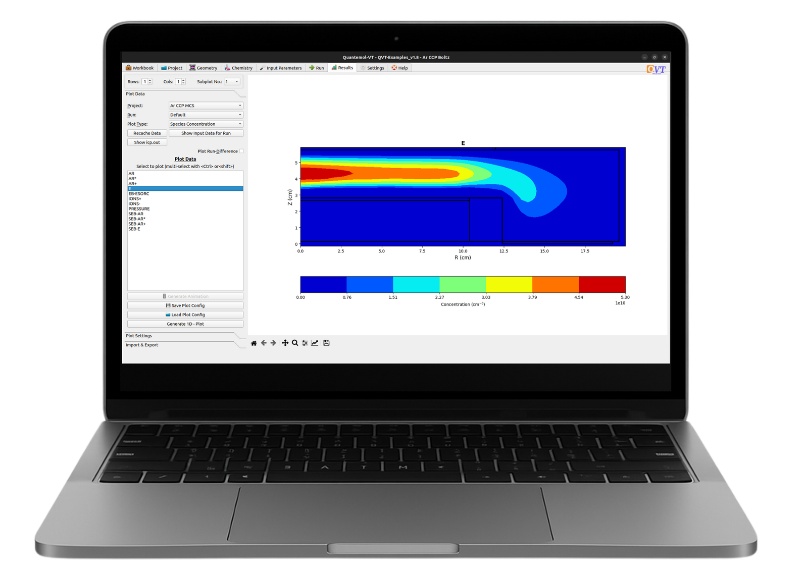
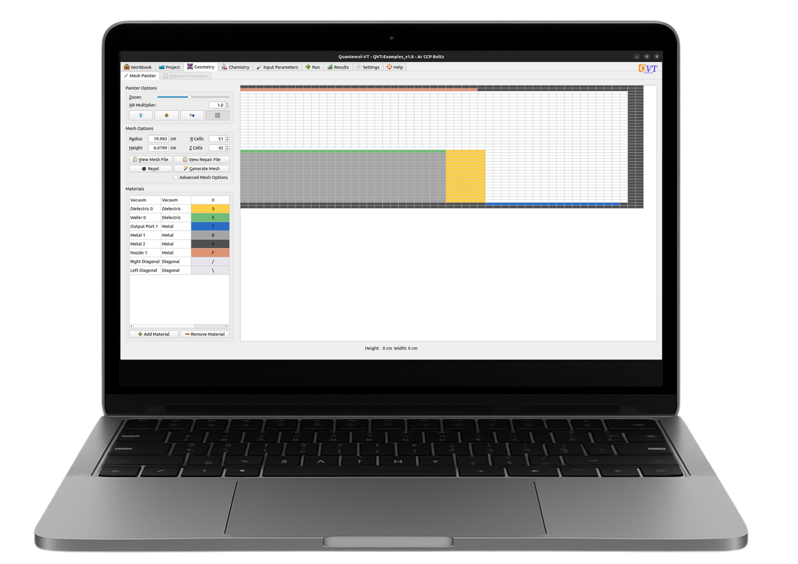
“QVT is a user-friendly front end to HPEM. Easy to define geometries. All HPEM features are available, integrated into one interface. Define reactor geometry, set input parameters… View output plasma parameters like concentrations, fluxes, temperatures.”
“QVT is a user-friendly front end to HPEM. Easy to define geometries. All HPEM features are available, integrated into one interface. Define reactor geometry, set input parameters… View output plasma parameters like concentrations, fluxes, temperatures.”


